
Η Taiwan Economic Daily he claims that the TSMC achieved a significant internal discovery for its final disposal lithography technology 2 nm.
ΣAccording to the publication, this milestone allows TSMC to is optimistic about an implementation of early production "Risk Production" 2 nm in 2023.
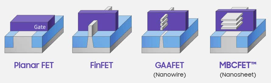
Still impressive are the reports that TSMC to abandon FinFet technology for a new multi-bridge channel field effect (MBCFET) transistor based on Gate-All-Around (GAA) technology. This important discovery is coming one year after the creation of an indoor team by TSMC, which aimed to pave the way for the development of 2 nm lithography.
MBCFET technology extends the GAAFET architecture by taking the Nanowire field-effect transistor and "spreading" it to become a Nanosheet. The main idea is to make the field-effect transistor XNUMXD.
This new complementary metal oxide semiconductor transistor can improve circuit control and reduce current leakage. This design philosophy is not exclusive to TSMC - Samsung plans to develop a variation of this design in their lithography technology 3 nm.

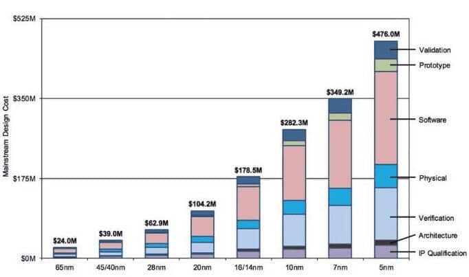
As usual, further reduction in chip manufacturing scale comes at a huge cost. Specifically, the development cost for the 5 nm lithograph has already reached $ 476 million, while Samsung states that the technology GAA of 3 nm will cost over $ 500 million. Of course, the development of lithography 2 nm, will exceed these amounts…
 Do not forget to follow it Xiaomi-miui.gr on Google News to be informed immediately about all our new articles!


